Datasheet explained · Texas Instruments · 3.3 V LDO · TLV74033
TLV740P Datasheet Explained: Specs, Pinout & Application Circuit
The TLV740P datasheet is short, but two lines in it change how you should use the chip: the EN pin and the junction-temperature limit. Here is everything you need, checked against TI’s latest revision.
Ramanu Systems · Pune, India · Based on TI datasheet SBVS401B (revised August 2025)
The TLV740P is a 300 mA general-purpose CMOS LDO from Texas Instruments. It takes 1.4 to 5.5 V in and gives a fixed 1.0 to 3.3 V out. The “P” means it has an active output discharge; the 3.3 V version is the TLV74033P. It is the modern, low-current replacement for the AMS1117 in most 5 V to 3.3 V jobs.
Is the TLV740P right for your design?
It’s a good fit if:
- You need 3.3 V for an ESP32, MCU or sensors from 5 V USB
- You’re replacing an AMS1117 and want lower dropout and idle current
- Your average load is around 150 mA or less from 5 V
- You run from a Li-ion cell (dropout 460 mV at 300 mA)
- You want the output to survive a short (folds back to 40 mA)
- You want a cheap, tiny, widely available part
Look elsewhere if:
- You power audio, RF or a precision ADC (noise is high; use a low-noise LDO)
- Your battery sleeps for months (50 µA idle adds up)
- Your input is above 5.5 V
- You need a full 300 mA continuously from 5 V in a small package
TLV740P key specifications
Typical values at 25 °C unless marked. LDO numbers depend on conditions, so they’re listed too.
| Parameter | Value | Condition / note |
|---|---|---|
| Input voltage | 1.4 to 5.5 V | 6.0 V absolute maximum |
| Output voltage | 1.0 to 3.3 V, fixed | 3.3 V = TLV74033 |
| Output current | 300 mA | Limited by heat in practice: see thermal |
| Output accuracy | ±1% | 25 °C, 1 mA load |
| Dropout voltage | 460 mV | 300 mA, outputs 2.1 to 3.3 V |
| Quiescent current | 50 µA (80 µA max) | No load |
| Shutdown current | 0.1 µA (1 µA max) | EN below 0.4 V |
| PSRR | 65 dB at 1 kHz | 32 dB at 1 MHz (5.4 V in, 3.3 V out, 150 mA) |
| Output noise | 65 µVrms | 100 Hz–100 kHz at 1.0 V out; higher at 3.3 V |
| Current limit | 360 mA, 40 mA into a short | Hybrid brick-wall and foldback |
| Start-up time | 100 µs | 1 µF output, 300 mA |
| Capacitors | 1 µF in, 1 to 100 µF out | At least 0.5 µF effective on the output |
| Thermal shutdown | 158 °C | Restarts at 140 °C |
| Junction temperature | −40 to 85 °C | Recommended operating range (125 °C absolute max) |
TLV740P pinout
The TLV740P comes in a hand-solderable SOT-23-5 and a 1×1 mm X2SON. The pin numbers differ between them, so check which one you’re drawing.
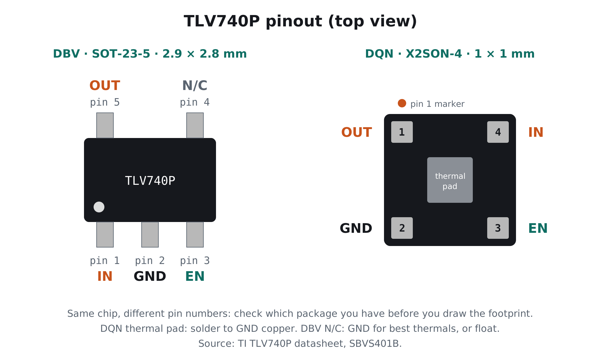
| Pin | SOT-23-5 (DBV) | X2SON-4 (DQN) | Function |
|---|---|---|---|
| IN | 1 | 4 | Input. 1 µF to GND, close to the pin. |
| GND | 2 | 2 | Ground |
| EN | 3 | 3 | Enable, active high. Do not float: tie to IN if unused. |
| OUT | 5 | 1 | Regulated output. 1 µF or more to GND. |
| N/C | 4 | – | Connect to GND for best heat spreading, or leave open |
| Thermal pad | – | pad | Solder to a large GND copper area |
TLV740P typical application circuit
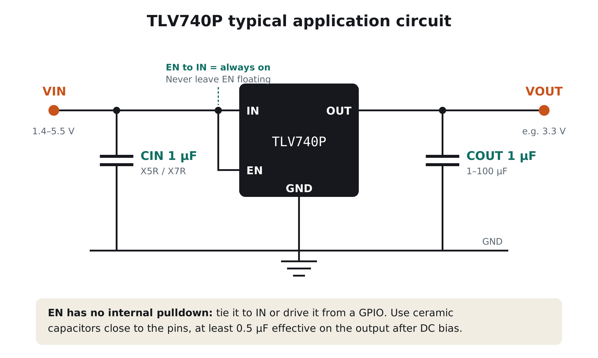
- Two ceramic capacitors1 µF from IN to GND and at least 1 µF from OUT to GND (up to 100 µF is stable). After DC-bias derating, the output must still have 0.5 µF. X5R or X7R, right at the pins.
- Tie EN somewhere, alwaysUnlike some newer TI LDOs, the TLV740P’s EN pin has no internal pulldown. TI’s pin table says plainly: don’t float it. Tie it to IN for always-on, or drive it from a GPIO (below 0.4 V is off).
- Give it copperThe SOT-23’s N/C pin can go to GND to help spread heat. On the X2SON, solder the thermal pad to a large ground area. You’ll see why in the next section.
How much current can it really deliver from 5 V?
This is the part most people miss. TI’s recommended operating range for the TLV740P’s junction is −40 to 85 °C, not the 125 °C many LDOs allow. An LDO turns its voltage drop into heat, P = (VIN − VOUT) × IOUT, and the SOT-23-5 has a thermal resistance of 216 °C/W on TI’s standard test board:
| 5 V → 3.3 V load | Heat in chip | Temperature rise | Junction at 25 °C room | Within 85 °C rating? |
|---|---|---|---|---|
| 100 mA | 0.17 W | ≈37 °C | ≈62 °C | Yes |
| 150 mA | 0.26 W | ≈55 °C | ≈80 °C | Just |
| 200 mA | 0.34 W | ≈73 °C | ≈98 °C | No |
| 300 mA | 0.51 W | ≈110 °C | ≈135 °C | No |
So on a small FR4 board, plan for roughly 150 mA continuous from 5 V at room temperature, and about 120 mA at 40 °C. That’s still plenty for an ESP32’s average current; Wi-Fi bursts are short. To use more, cut the heat: feed it from a lower voltage (from a 4.2 V Li-ion cell, 300 mA is only 0.27 W), add copper, or use a metal-core board. Our aluminium vs FR4 thermal test runs two TLV740P modules at exactly 5 V and 300 mA, on video.
TLV740P vs AMS1117
Both turn 5 V into 3.3 V on countless boards. The AMS1117 still wins on input voltage and current; the TLV740P wins almost everywhere else:
| TLV740P (3.3 V) | AMS1117-3.3 | |
|---|---|---|
| Dropout | 460 mV at 300 mA | About 1.1 V |
| Idle current | 50 µA | About 5 mA (100× more) |
| Output capacitor | 1 µF ceramic | Typically 22 µF, often tantalum |
| Max input | 5.5 V | Up to 15 V |
| Max current | 300 mA | About 1 A |
| Package | SOT-23-5 / 1×1 mm | SOT-223 (better heat sinking) |
In practice: if your input is 5 V USB or a battery and your average load is modest, the TLV740P stays in regulation longer when USB sags and doesn’t drain a battery while idle. If you feed from 9–12 V or need 500 mA+, the TLV740P isn’t the right part. Our full AMS1117 vs TLV740P comparison goes deeper.
Skip the SMD soldering
TrueVolt74033: the TLV740P on a ready module
The 3.3 V module the AMS1117 should have been, at a similar price to a generic board.
- Genuine TI TLV740P from authorised distribution
- 0.46 V dropout: no resets when USB sags
- Survives shorts (foldback to 40 mA, thermal shutdown)
- Aluminium PCB to carry heat away, reverse-current Schottky
- Designed & made in Pune, India
TLV740P alternatives
| Part | Choose it when |
|---|---|
| TPS7A20 | The rail feeds audio, RF or an ADC and noise matters (7 µVrms). Ours: TrueVolt LN-7A2033 |
| TPS7A03 | Battery life comes first: 200 nA idle. Ours: TrueVolt NP-7A0333 |
| AMS1117 | You need more than 5.5 V in or more than 300 mA, and idle current doesn’t matter |
| Buck converter | You need 500 mA+ from 5 V and heat is the problem |
For engineers: the finer print
1. Foldback starts early
The current limit is a hybrid: about 360 mA as a brick wall, then folding back as the output falls, down to 40 mA into a dead short. TI puts the foldback point at 95% of the nominal output. A load that pulls a big start-up surge (a large capacitor bank, a motor, a Wi-Fi module charging its bulk capacitor) can pull the output just low enough to enter foldback and stay there. If a board “won’t start” on a TLV740P but works on a bench supply, this is the first suspect.
2. Fast start-up means inrush
Start-up is about 100 µs. Charging 100 µF to 3.3 V that fast needs over 3 A in theory, so the current limit, not the soft-start, sets the ramp. Keep downstream bulk capacitance sensible, or bring loads up after the rail with a load switch.
3. PSRR and noise are ordinary
65 dB at 1 kHz falls to 32 dB at 1 MHz, so charger and buck-converter ripple passes through with only about 40× attenuation. That’s fine for digital logic, not for a 24-bit ADC or a microphone preamp.
Frequently asked questions
What is the TLV740P?
The TLV740P is a 300 mA CMOS LDO linear regulator from Texas Instruments with 1.4 to 5.5 V input, fixed 1.0 to 3.3 V output, 460 mV dropout at full load, 50 µA quiescent current and an active output discharge. The 3.3 V version is the TLV74033P.
What is the TLV740P pinout?
In SOT-23-5: pin 1 IN, pin 2 GND, pin 3 EN, pin 4 no connection, pin 5 OUT. In the 1×1 mm X2SON-4: pin 1 OUT, pin 2 GND, pin 3 EN, pin 4 IN, plus a thermal pad soldered to ground.
Can I leave the TLV740P EN pin floating?
No. The EN pin has no internal pulldown, and TI says not to leave it floating. Tie it to IN for an always-on rail, or drive it from a GPIO; below 0.4 V turns the regulator off.
What is the difference between TLV740 and TLV740P?
The TLV740P adds an active output discharge: when it is disabled, a pulldown of about 120 Ω empties the output capacitor so the rail falls quickly to 0 V.
Can the TLV740P replace an AMS1117?
For 5 V or battery to 3.3 V at moderate current, yes: it has less than half the dropout, about 100 times lower idle current and needs only a 1 µF ceramic output capacitor. It cannot replace an AMS1117 fed from more than 5.5 V or loaded above 300 mA.
How much current can the TLV740P supply from 5 V?
Its rating is 300 mA, but TI’s recommended junction range ends at 85 °C. From 5 V to 3.3 V in SOT-23-5 on a standard test board, that allows roughly 150 mA continuous at 25 °C and about 120 mA at 40 °C. More copper, a metal-core PCB or a lower input voltage raise the limit.
Build with it today
The AMS1117 upgrade, ready to plug in
Genuine TI TLV740P on an aluminium board, short-circuit safe. Made in India.