Datasheet explained · Texas Instruments · Low-noise LDO · TPS7A2033
TPS7A20 Datasheet Explained: Specs, Pinout & Application Circuit
The TPS7A20 datasheet runs to dozens of pages. Here is what you actually need to design with it, on one page, with every number checked against TI’s latest revision.
Ramanu Systems · Pune, India · Based on TI datasheet SBVS338H (revised July 2024)
The TPS7A20 is a 300 mA, ultra-low-noise linear regulator (LDO) from Texas Instruments. It takes 1.6 to 6.0 V in and gives a fixed 0.8 to 5.5 V out. The 3.3 V version is the TPS7A2033. It needs only two 1 µF ceramic capacitors and no noise-bypass capacitor.
Is the TPS7A20 right for your design?
It’s a good fit if:
- You power an ADC, sensor, microphone or DAC and need a quiet rail
- Your input is 5 V USB, a Li-ion cell or a 3.6 V rail
- Your load is under about 250 mA
- You want low idle current (6.5 µA) for battery products
- Board space is tight (1×1 mm package available)
- You want few parts: two 1 µF capacitors, nothing else
Look elsewhere if:
- You need more than 300 mA
- Your input is above 6 V (12 V, 9 V battery)
- You need a precision voltage reference (it’s ±1.5%)
- Your battery sleeps for months (look at nano-amp LDOs)
TPS7A20 key specifications
Typical values at 25 °C unless marked max. Conditions matter for an LDO, so they’re listed with each number.
| Parameter | Value | Condition / note |
|---|---|---|
| Input voltage | 1.6 to 6.0 V | 6.5 V absolute maximum. Don’t design to it. |
| Output voltage | 0.8 to 5.5 V, fixed | Many factory options, including 1.8, 2.5, 2.8, 3.0, 3.3 and 5.0 V |
| Output current | 300 mA | Limited by heat in practice: see thermal |
| Output noise | 7 µVrms | 10 Hz to 100 kHz, 2.8 V out, 300 mA (10 µVrms at 1 mA). No bypass capacitor. |
| PSRR | 95 dB at 1 kHz | 20 mA load; falls to 45 dB at 1 MHz. See the chart. |
| Dropout voltage | 140 mV max (145 mV in SOT-23) | 300 mA, output 2.5 to 5.5 V |
| Quiescent current | 6.5 µA | No load; 8.5 µA max at 25 °C, 15 µA max at 125 °C |
| Shutdown current | 0.07 µA | EN low; 0.2 µA max |
| Output accuracy | ±1.5% max | Over line, load and temperature (outputs ≥1.85 V; ≥2.8 V in SOT-23) |
| Current limit | 520 mA typ, 360 mA min | Folds back to about 160 mA into a short |
| Capacitors | 1 µF in, 1 µF out | Output: 0.47 to 200 µF effective, ESR under 100 mΩ |
| Thermal shutdown | 165 °C | Restarts at 140 °C |
| Junction temperature | −40 to 125 °C | Recommended operating range |
TPS7A20 pinout
The TPS7A20 comes in four packages, and the pin numbers are different in each. The two you’re most likely to use are the SOT-23-5 (easy to hand-solder) and the 1×1 mm X2SON (for tight boards; it needs reflow assembly).
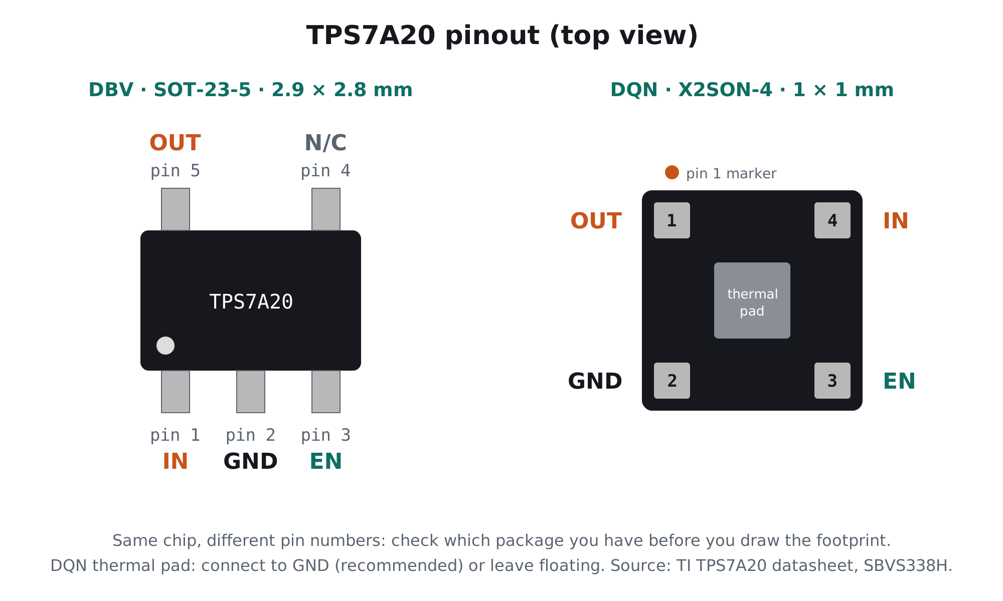
| Pin | SOT-23-5 (DBV) | X2SON-4 (DQN) | DSBGA-4 (YCK / YCJ) | Function |
|---|---|---|---|---|
| IN | 1 | 4 | A1 | Input supply. 1 µF to GND, close to the pin. |
| GND | 2 | 2 | B2 | Ground |
| EN | 3 | 3 | B1 | Enable. High (above 0.9 V) = on. Internal pulldown keeps it off if floating. |
| OUT | 5 | 1 | A2 | Regulated output. 1 µF to GND, close to the pin. |
| N/C | 4 | – | – | No internal connection |
| Thermal pad | – | pad | – | Connect to GND copper with vias (or leave floating) |
TPS7A20 typical application circuit
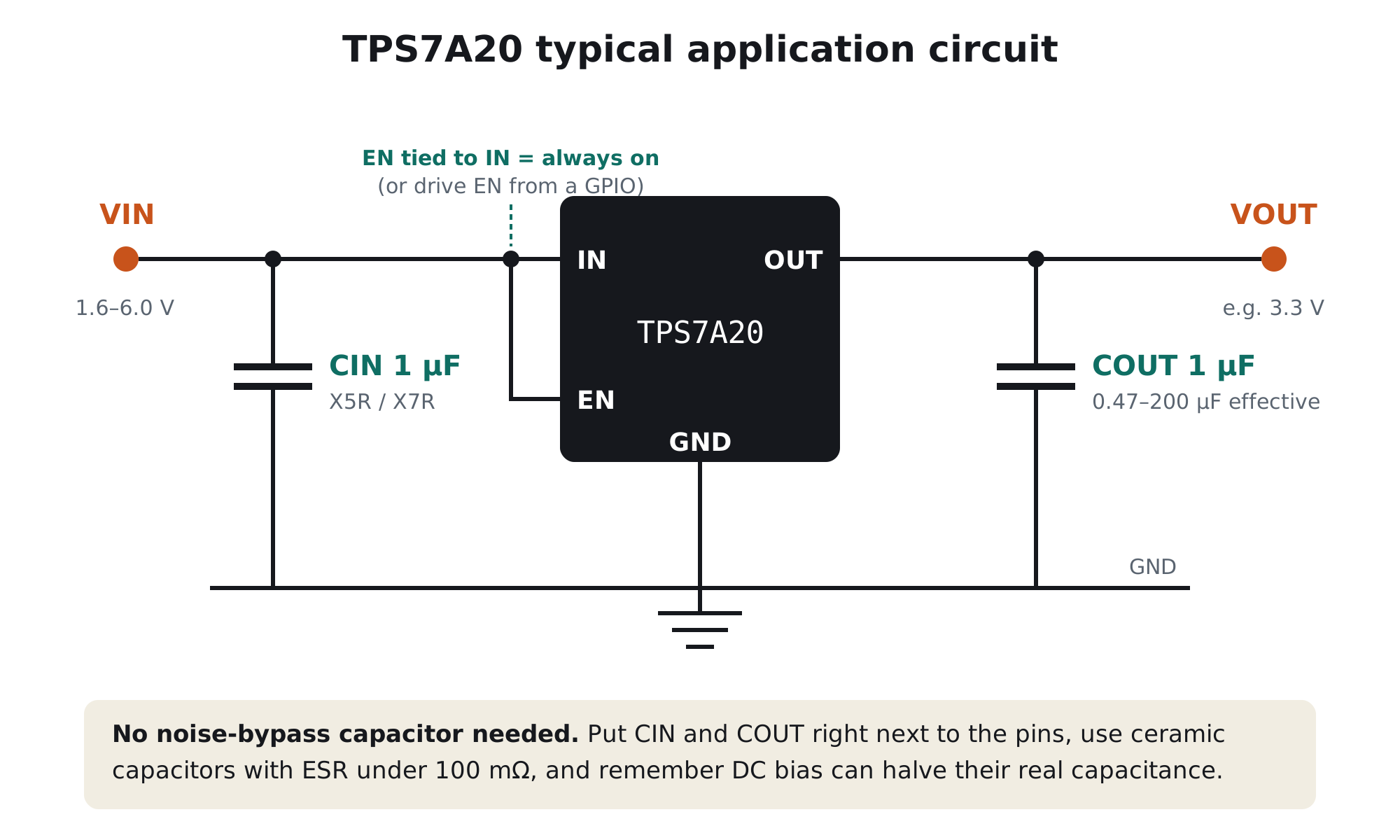
This is one of the simplest LDO circuits you’ll draw. Three steps:
- Two 1 µF ceramic capacitorsOne from IN to GND, one from OUT to GND. Use X5R or X7R, placed right next to the pins. There’s no noise-reduction pin, so there’s no third capacitor.
- Decide what EN doesTie EN to IN for an always-on rail. To switch the rail from a microcontroller, drive EN from a GPIO: above 0.9 V turns it on, below 0.3 V turns it off. A floating EN stays off, thanks to the internal pulldown.
- Give it copperUse wide traces or planes for IN, OUT and GND, and put a few thermal vias around the package. On the X2SON, solder the thermal pad to a ground area with vias.
Capacitors: the part most people get wrong
TI asks for at least 0.47 µF of effective output capacitance, and warns that DC bias and temperature can cut a ceramic capacitor’s real value by about half. A “1 µF” 0402 capacitor sitting at 3.3 V can be close to that limit. Use a larger case size or a higher value if you have room. Our MLCC DC bias article shows how much capacitance you really get from 0603, 0805 and 1206 parts.
How much current can it really deliver?
The datasheet says 300 mA, but an LDO turns the voltage it drops into heat: P = (VIN − VOUT) × IOUT. From 5 V to 3.3 V, that’s 1.7 V × current. Using TI’s thermal resistance figures (187 °C/W for SOT-23-5 on the standard JEDEC test board):
| Input → output | Load | Heat in chip | Temperature rise (SOT-23) | Verdict |
|---|---|---|---|---|
| 5 V → 3.3 V | 100 mA | 0.17 W | ≈32 °C | Easy |
| 5 V → 3.3 V | 200 mA | 0.34 W | ≈64 °C | Fine |
| 5 V → 3.3 V | 300 mA | 0.51 W | ≈95 °C | Too hot above ~30 °C ambient |
| 4.2 V Li-ion → 3.3 V | 300 mA | 0.27 W | ≈51 °C | Fine |
At 40 °C ambient (a normal Indian summer indoors), staying under the 125 °C junction limit from 5 V works out to about 270 mA continuous in SOT-23 on a JEDEC board. More copper, thermal vias or an aluminium (metal-core) PCB lower the temperature rise. Our aluminium vs FR4 LDO thermal test shows the difference on video.
What 95 dB PSRR really means
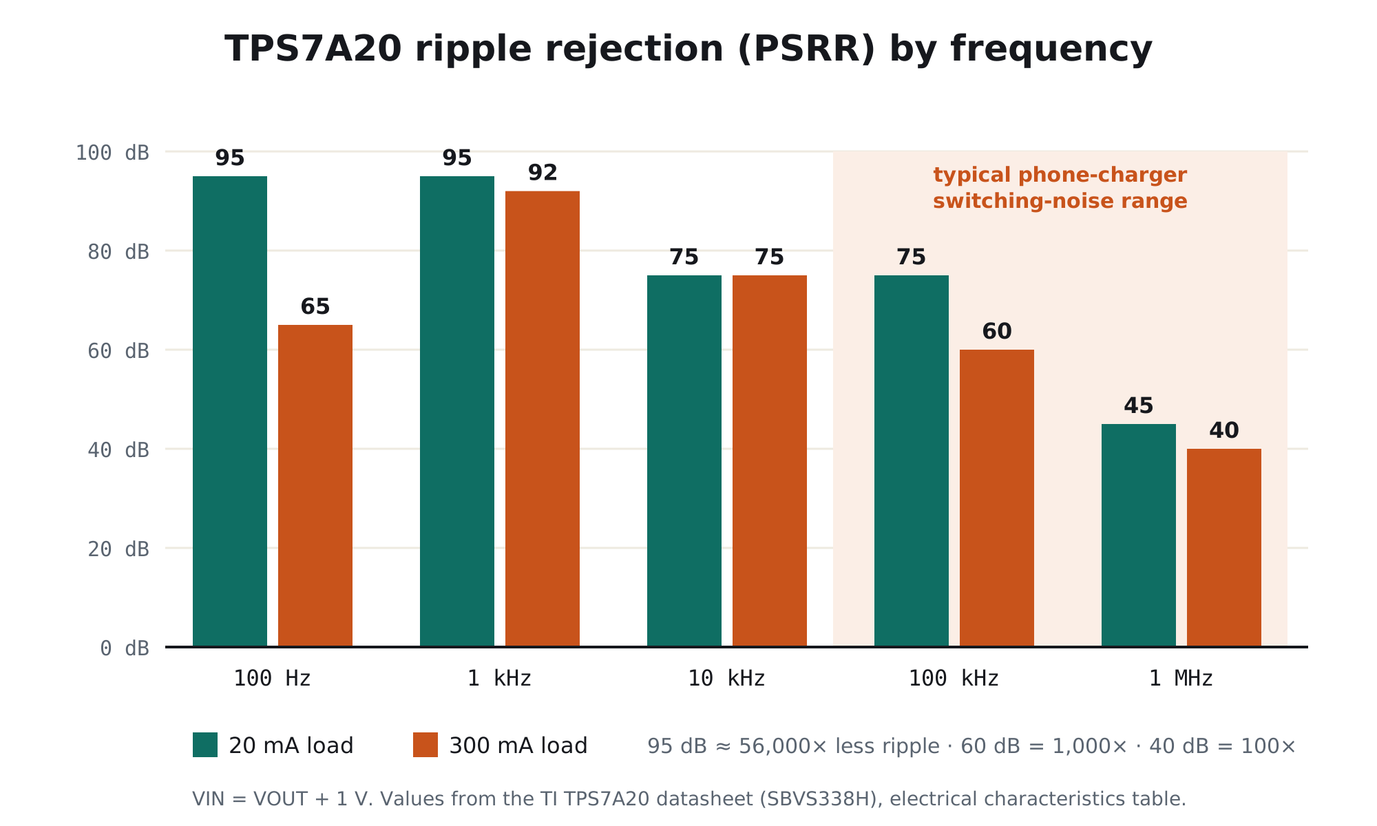
PSRR is how much of the ripple on the input makes it to the output. 95 dB means the ripple is cut about 56,000 times. But the number in the headline is measured at 1 kHz with a light load. Phone chargers and switching regulators make their noise at 50 kHz to a few MHz, where PSRR is lower:
Skip the SMD soldering
TPS7A2033, ready to use on a module
Prototyping, or just need a clean 3.3 V rail without laying out a board? We put the genuine TI TPS7A2033 on two breadboard-friendly modules, with the capacitors, filtering and protection already done.
- TrueVolt LN-7A2033: 3 pins (VIN, GND, VOUT). Feed it 5 V, get a quiet 3.3 V
- PureRail C33 Nano: USB-C in, filtered 5 V + low-noise 3.3 V out
- Ferrite-bead filtering in front of the LDO for charger noise
- Samsung capacitors, aluminium PCB, reverse-polarity protection
- Genuine TI silicon from authorised distribution. Designed & made in Pune, India
TPS7A20 alternatives
| Part | Choose it when |
|---|---|
| TLV773 | TI’s pin-compatible, lower-cost option for circuits that are less sensitive to noise |
| TPS7A20L | You need the enable pin to work with 1.2 V logic |
| TPS7A03 | Battery life comes first: idles in the nano-amp range. Ours: TrueVolt NP-7A0333 |
| TLV740P | General 3.3 V power for MCUs where noise isn’t critical. Ours: TrueVolt74033 |
For engineers: the finer print in the datasheet
1. Noise is lower at full load
TI specifies 7 µVrms at 300 mA and 10 µVrms at 1 mA (10 Hz–100 kHz, 2.8 V out). Either way it’s far below one LSB of a 16-bit ADC on a 3.3 V range (about 50 µV). Noise is specified without a noise-reduction capacitor because the TPS7A20 doesn’t have an NR pin.
2. PSRR drops with load at low frequency
At 100 Hz, PSRR is 95 dB at 20 mA but 65 dB at 300 mA. If mains-frequency ripple from a linear supply matters to you, keep some headroom (TI’s figures use VIN = VOUT + 1 V) and don’t run right at full load.
3. Start-up, enable and UVLO
| Behaviour | Datasheet value |
|---|---|
| Start-up time (EN high to 95% of VOUT) | 750 to 1150 µs, internal soft-start limits inrush |
| EN thresholds | On above 0.9 V, off below 0.3 V |
| Smart-enable pulldown | About 500 kΩ, released once EN is high; EN leakage 90 nA typ |
| Undervoltage lockout | 1.35 V rising, 1.3 V falling (typ) |
| Active output discharge | About 150 Ω pulldown on OUT when disabled (versions with the discharge option) |
4. Current limit and short circuit
The limit is a brick wall (520 mA typ, 360 mA min) until the output collapses, then it folds back to about 160 mA into a dead short. That protects the chip, but a load that needs a big start-up surge (large capacitors, a motor) can get stuck in foldback. Bring such loads up slowly or switch them in after the rail is up.
Frequently asked questions
What is the TPS7A20?
The TPS7A20 is a 300 mA ultra-low-noise LDO linear regulator from Texas Instruments. It accepts 1.6 to 6.0 V, outputs a fixed 0.8 to 5.5 V, has 7 µVrms output noise, 95 dB PSRR at 1 kHz and 6.5 µA quiescent current. The TPS7A2033 is the 3.3 V version.
What is the TPS7A20 pinout?
In SOT-23-5 (DBV): pin 1 IN, pin 2 GND, pin 3 EN, pin 4 no connection, pin 5 OUT. In X2SON-4 (DQN): pin 1 OUT, pin 2 GND, pin 3 EN, pin 4 IN, plus a thermal pad that should go to ground.
What capacitors does the TPS7A20 need?
A 1 µF ceramic capacitor on the input and a 1 µF ceramic capacitor on the output. The output needs at least 0.47 µF of effective capacitance after DC bias derating and an ESR below 100 mΩ. X5R or X7R types work well. No noise-bypass capacitor is required.
Can I leave the TPS7A20 EN pin floating?
No, not if you want the output on. EN has an internal pulldown, so a floating EN keeps the regulator off. Tie EN to IN for an always-on rail, or drive it from a GPIO (above 0.9 V is on).
What is the TPS7A20 dropout voltage?
140 mV maximum at 300 mA for outputs from 2.5 to 5.5 V (145 mV in the SOT-23-5 package). For example, the TPS7A2033 keeps regulating 3.3 V down to an input of roughly 3.45 V at full load.
Can the TPS7A2033 supply 300 mA from 5 V?
Electrically yes, but it gets hot: it dissipates about 0.5 W, which raises a SOT-23-5 on a standard test board by roughly 95 °C. At 40 °C ambient, plan for about 270 mA continuous, or improve cooling with more copper, thermal vias or an aluminium PCB.
Is there a ready-made TPS7A2033 module?
Yes. The Ramanu Systems TrueVolt LN-7A2033 is a three-pin TPS7A2033 module (VIN, GND, VOUT) with ferrite filtering and reverse-polarity protection, and the PureRail C33 Nano adds a USB-C input with a filtered 5 V output. Both use genuine TI parts and are made in Pune, India.
Build with it today
The TPS7A2033, already on a board
Plug it into a breadboard, feed it 5 V, and get the quiet 3.3 V this datasheet promises. Genuine TI, made in India.